
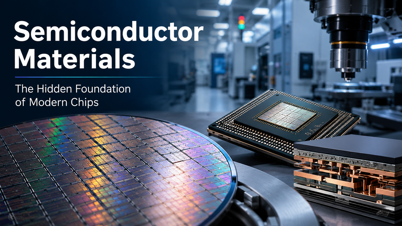
Semiconductor Materials: The Hidden Foundation of Modern Chips
Semiconductor materials are the physical foundation of the digital world. Every smartphone, laptop, electric vehicle, data center, solar inverter, medical device, satellite, and artificial intelligence system depends on materials that can control the flow of electricity with extraordinary precision.
When people talk about semiconductors, they often focus on chip brands, manufacturing nodes, AI processors, or supply chains. But behind every advanced chip is a much deeper materials story. Silicon wafers, photoresists, dielectric films, metal interconnects, compound semiconductors, substrates, dopants, packaging materials, and thermal interface materials all determine how fast, efficient, reliable, and scalable modern electronics can become.
The Semiconductor Industry Association notes that semiconductors are now essential building blocks for technologies such as artificial intelligence, quantum computing, advanced communications networks, and defense systems. Source: Semiconductor Industry Association
Technical Brief: Semiconductor materials are not just “chip ingredients.” They define transistor performance, power efficiency, heat management, manufacturing yield, device reliability, packaging density, and the long-term roadmap of computing hardware.
What Are Semiconductor Materials?
Semiconductor materials are materials whose electrical conductivity sits between conductors and insulators. This means they can be engineered to conduct electricity under specific conditions. That controllability makes them ideal for transistors, diodes, sensors, memory devices, lasers, power electronics, and integrated circuits.
The most famous semiconductor material is silicon. Silicon became dominant because it is abundant, stable, relatively inexpensive, and compatible with silicon dioxide, which helped enable reliable transistor manufacturing. However, modern semiconductor technology uses far more than silicon alone.
Today’s chip ecosystem depends on a sophisticated material stack. A single advanced chip may involve semiconductor crystals, insulating dielectrics, conductive metals, ultra-thin barrier layers, advanced photoresists, specialty gases, polishing materials, packaging substrates, underfills, adhesives, and heat-dissipation materials.
In other words, a semiconductor chip is not simply a piece of silicon. It is a precisely engineered materials system built layer by layer at microscopic and nanometer scale.
Why Semiconductor Materials Matter
Semiconductor performance is not determined only by circuit design. Materials influence almost every important chip metric: switching speed, leakage current, breakdown voltage, thermal conductivity, carrier mobility, defect density, reliability, and manufacturing yield.
As chips become smaller and more complex, materials become even more important. At advanced process nodes, tiny defects can cause performance loss or yield problems. At the same time, AI accelerators, electric vehicles, 5G infrastructure, and high-performance computing create demand for chips that handle more power, more heat, and more data.
This is why the semiconductor industry continuously searches for better materials. The goal is not only to make chips smaller. It is also to make them faster, cooler, more energy-efficient, more reliable, and easier to manufacture at scale.
The Semiconductor Material Stack
A useful way to understand semiconductor materials is to divide them by function. Some materials form the active device itself. Others insulate, connect, pattern, protect, package, or cool the chip.
| Material Category | Examples | Role in Semiconductor Devices |
|---|---|---|
| Base Semiconductor Materials | Silicon, silicon carbide, gallium nitride, gallium arsenide | Provide the active electronic properties for transistors, diodes, sensors, and power devices. |
| Dielectric Materials | Silicon dioxide, silicon nitride, high-k dielectrics | Provide insulation, gate control, isolation, and capacitance management. |
| Conductive Materials | Copper, tungsten, cobalt, ruthenium, aluminum | Create interconnects, contacts, electrodes, and power delivery paths. |
| Lithography Materials | Photoresists, anti-reflective coatings, developers | Enable microscopic pattern transfer during chip manufacturing. |
| Packaging Materials | Substrates, underfills, solder bumps, adhesives, thermal interface materials | Connect, protect, and cool chips after wafer fabrication. |
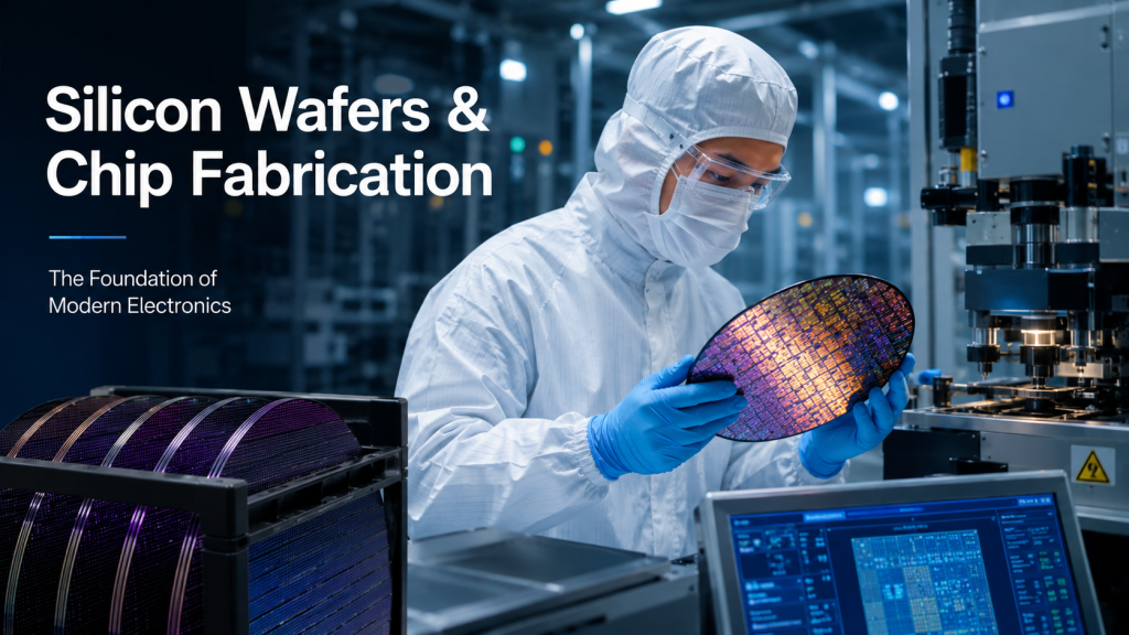
Silicon: Still the Core Material of the Chip Industry
Silicon remains the most important semiconductor material in the world. Its dominance comes from a combination of technical, economic, and manufacturing advantages. Silicon wafers can be produced at extremely high purity, processed at scale, and integrated into mature manufacturing flows.
Silicon also supports complementary metal-oxide-semiconductor technology, commonly known as CMOS. CMOS is the foundation of modern logic chips, microprocessors, memory, image sensors, and many integrated circuits.
Even as new materials enter the industry, silicon is not disappearing. Instead, the industry is adding new materials around silicon to extend performance. High-k dielectrics, metal gates, strained silicon, advanced interconnect metals, and new packaging materials have all helped keep silicon technology competitive.
Intel has highlighted several foundational process innovations in modern CMOS, including strained silicon, high-k metal gates, FinFETs, RibbonFET, and backside power delivery technologies. Source: Intel
Compound Semiconductors: Beyond Silicon
Compound semiconductors are made from two or more elements. Unlike silicon, which is a single-element semiconductor, compound semiconductors can offer special properties such as higher electron mobility, wider bandgaps, better high-frequency performance, or superior power handling.
Important compound semiconductor materials include gallium nitride, silicon carbide, gallium arsenide, indium phosphide, and related alloys. These materials are especially important in power electronics, radio-frequency devices, optoelectronics, LEDs, lasers, and high-speed communications.
The reason is simple: not every application needs the same kind of semiconductor. A smartphone processor needs dense logic. An electric vehicle inverter needs high-voltage efficiency. A 5G base station needs high-frequency performance. A laser diode needs efficient light emission. Different materials solve different engineering problems.
Engineering View: Silicon is excellent for mainstream computing, but materials such as silicon carbide and gallium nitride are increasingly important where power density, thermal performance, high voltage, and high-frequency operation matter.
Silicon Carbide: A Key Material for Power Electronics
Silicon carbide, often written as SiC, is a wide-bandgap semiconductor material. Compared with silicon, SiC can operate at higher voltages, higher temperatures, and higher power levels. This makes it valuable for electric vehicles, renewable energy systems, industrial motor drives, fast chargers, and power grids.
In electric vehicles, SiC power devices can improve inverter efficiency and help reduce energy losses. In solar and wind systems, SiC can support more efficient power conversion. In industrial applications, it can help reduce heat and improve system performance.
However, SiC is more difficult and expensive to manufacture than silicon. Crystal growth, wafer quality, defect control, device processing, and packaging are all challenging. The industry is working to improve wafer size, reduce defects, and lower costs so SiC can scale more broadly.
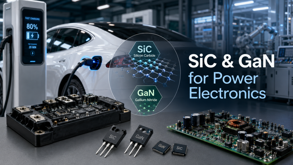
Gallium Nitride: High-Speed Power and RF Performance
Gallium nitride, or GaN, is another wide-bandgap semiconductor. It is known for high electron mobility, fast switching, and strong performance in high-frequency and power applications. GaN is used in radio-frequency systems, fast chargers, power adapters, data center power conversion, radar, satellite communications, and 5G infrastructure.
GaN power devices can switch faster than traditional silicon power devices, which can reduce energy loss and allow smaller power systems. This is one reason GaN has become increasingly visible in compact chargers and high-efficiency power electronics.
Reuters reported in 2025 that an MIT spinout, Vertical Semiconductor, is developing gallium nitride power chip technology designed to improve electricity delivery efficiency for AI servers, highlighting GaN’s relevance to data center power challenges. Source: Reuters
High-k Dielectrics and Gate Materials
As transistors became smaller, traditional silicon dioxide gate dielectrics became too thin to control leakage effectively. This pushed the industry toward high-k dielectric materials and metal gate stacks.
High-k materials allow better electrostatic control while reducing leakage current compared with ultra-thin silicon dioxide. Metal gates help tune transistor work functions and improve performance. Together, high-k metal gate technology became a critical step in extending CMOS scaling.
Intel documented high-k and metal gate technology as a major CMOS advancement, showing how new gate stacks helped address leakage and performance challenges in advanced transistors. Source: Intel high-k gate dielectric paper
This example shows why semiconductor materials matter. A change in one thin layer of material can reshape the future of transistor scaling.
Interconnect Materials: The Wiring Problem Inside Chips
Transistors receive most of the attention, but interconnects are equally important. Interconnects are the tiny wires that connect billions of transistors inside a chip. As chips become denser, wiring becomes a major performance bottleneck.
Copper has been widely used for interconnects because of its low electrical resistance. However, at very small dimensions, interconnect resistance, capacitance, electromigration, and reliability become serious challenges. Barrier materials, liners, low-k dielectrics, and alternative metals become increasingly important.
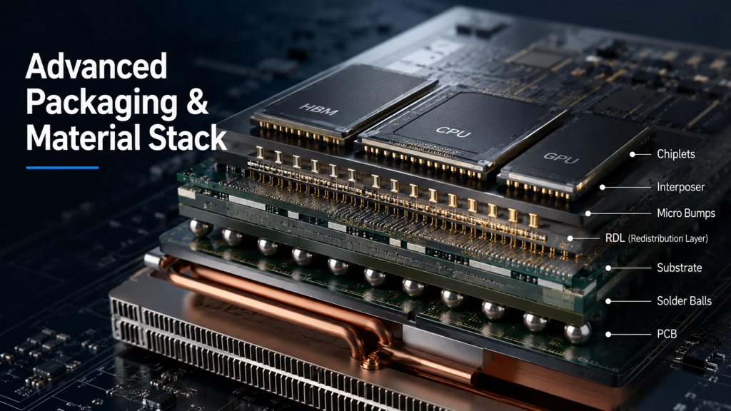
The interconnect problem is one reason advanced packaging has become so important. Instead of relying only on shrinking transistors, the industry is also improving how chips are connected to each other through chiplets, interposers, 2.5D packaging, 3D stacking, and advanced substrates.
Lithography Materials: Patterning the Nanoscale World
Lithography materials are essential for defining chip patterns. Photoresists are light-sensitive materials used to transfer circuit patterns onto wafers. As semiconductor manufacturing moves to smaller dimensions, photoresist performance becomes increasingly difficult and important.
Extreme ultraviolet lithography, or EUV, requires highly specialized materials. EUV photoresists must balance sensitivity, resolution, line-edge roughness, and defect control. This is not easy. At advanced nodes, small patterning errors can reduce yield or damage device performance.
The lithography material supply chain is also strategically important. Photoresists, developers, specialty gases, and cleaning chemicals must meet extreme purity and consistency requirements. Semiconductor manufacturing is one of the most demanding chemical-processing environments in the world.
Packaging Materials: Where Performance Is Increasingly Won
Advanced packaging is becoming a major performance frontier. As monolithic chip scaling becomes more difficult and expensive, chipmakers increasingly use packaging technologies to connect multiple dies, memory stacks, and accelerators in one system.
This shift makes packaging materials more important. Substrates, redistribution layers, solder materials, underfills, adhesives, thermal interface materials, and encapsulants all influence signal integrity, heat dissipation, mechanical reliability, and manufacturing yield.
AI chips and high-performance computing systems are especially demanding. They require high-bandwidth memory, dense interconnects, advanced substrates, and strong thermal management. In many systems, the package is no longer just a protective shell. It is part of the performance architecture.
Thermal Materials: Managing Heat in the AI Era
Heat has become one of the biggest constraints in modern electronics. AI accelerators, power devices, 5G systems, and high-density servers generate significant thermal loads. If heat is not managed properly, performance drops and device reliability suffers.
Thermal interface materials, heat spreaders, advanced substrates, diamond-like materials, ceramics, and liquid-cooling-compatible package designs are becoming more important. The goal is to move heat away from active devices as efficiently as possible.
This is especially important for data centers. AI workloads require large amounts of computing power, and power delivery losses can become costly. Better materials can improve electrical efficiency and reduce thermal stress across the system.
2D Materials and the Future Logic Roadmap
As transistor scaling approaches physical limits, researchers are exploring new channel materials. Two-dimensional materials, such as molybdenum disulfide and tungsten diselenide, are especially interesting because they can be extremely thin while maintaining useful electronic properties.
Imec describes 2D materials as a promising option for future logic scaling, especially in advanced device architectures such as CFETs. However, imec also notes that major development is still needed before broad industrial adoption. Source: imec
The promise of 2D materials is significant, but the challenges are equally serious. These include wafer-scale deposition, defect control, contact resistance, integration with existing process flows, reliability, and manufacturability on 300mm wafers.
In professional terms, 2D materials are not a short-term replacement for silicon. They are a potential long-term extension of the logic roadmap if the industry can solve the integration and manufacturing problems.
Materials Supply Chains and Geopolitical Risk
Semiconductor materials are also a supply-chain issue. Advanced chips require high-purity chemicals, specialty gases, rare metals, wafers, substrates, and precision materials from a global supplier network. Even small disruptions can affect production schedules and costs.
Materials such as gallium and germanium have received more attention because they are important for compound semiconductors and optoelectronic applications. Export restrictions, geopolitical tensions, and concentrated supply chains can create uncertainty for manufacturers.
This is why countries and companies are investing in supply-chain resilience. The goal is not only to build more fabs. It is also to secure the materials, chemicals, equipment, and talent needed to run those fabs reliably.
Quality, Purity, and Defect Control
Semiconductor manufacturing requires extreme purity. Contamination at tiny concentrations can create defects, reduce yield, or cause reliability failures. This applies to wafers, gases, chemicals, photoresists, metals, and packaging materials.
Defect control is especially important because advanced chips contain billions of devices. A single defect in a critical location can cause a circuit failure. As geometries shrink, the tolerance for particles, impurities, roughness, and variability becomes much smaller.
For material suppliers, this creates a high barrier to entry. It is not enough to produce a material with the right chemical formula. The material must meet strict purity, consistency, traceability, and process-compatibility requirements.
How Semiconductor Materials Shape Emerging Technologies
The future of many industries depends on semiconductor materials. Artificial intelligence requires advanced logic, memory, packaging, and thermal materials. Electric vehicles require power semiconductors such as SiC and GaN. Renewable energy systems need efficient inverters and grid electronics. 5G and future 6G networks depend on RF materials. Quantum computing requires specialized materials and fabrication methods.
This means semiconductor materials are not only an engineering topic. They are an economic and strategic topic. The countries and companies that control advanced materials capabilities may gain advantages in computing, energy, defense, communications, and industrial automation.
Key Challenges in Semiconductor Materials
The semiconductor materials industry faces several major challenges. The first is scaling. A material that works in a laboratory must eventually work across high-volume manufacturing lines with stable yield and predictable cost.
The second challenge is integration. A new material must be compatible with existing process flows, thermal budgets, contamination rules, equipment, and device architectures. Many promising materials fail not because they lack good properties, but because they are too difficult to integrate.
The third challenge is cost. Advanced materials often require expensive production methods, tight process control, and complex qualification cycles. Chipmakers will only adopt new materials when the performance benefit justifies the risk and cost.
The fourth challenge is reliability. Semiconductor devices must operate for years under electrical, thermal, and mechanical stress. Materials must remain stable under real-world conditions, not just during early lab tests.
Future Outlook: Materials Innovation Will Drive the Next Chip Era
The future of semiconductors will not be driven by transistor scaling alone. It will be driven by a combination of new materials, new device structures, new packaging methods, better thermal management, and more resilient supply chains.
Silicon will remain central, but the surrounding material ecosystem will continue to expand. Silicon carbide and gallium nitride will grow in power and RF applications. High-k dielectrics and advanced metals will remain essential for transistor engineering. Packaging materials will become more important for AI and high-performance computing. 2D materials may open future options for logic scaling if manufacturing challenges can be solved.
For businesses, investors, engineers, and technology observers, semiconductor materials deserve more attention. They are often invisible to consumers, but they decide what chips can actually do.
FAQ: Semiconductor Materials
What is the most common semiconductor material?
Silicon is the most common semiconductor material because it is abundant, stable, scalable, and deeply integrated into modern chip manufacturing.
Why are silicon carbide and gallium nitride important?
Silicon carbide and gallium nitride are wide-bandgap materials that can support high power, high voltage, high temperature, and fast switching. They are important for electric vehicles, chargers, renewable energy, data centers, RF systems, and industrial electronics.
Are semiconductor materials only used in computer chips?
No. They are used in power electronics, sensors, LEDs, lasers, solar cells, communication systems, automotive electronics, medical devices, and industrial equipment.
Will new materials replace silicon?
Not broadly in the near term. Silicon will remain dominant in mainstream logic and memory, while new materials will complement silicon in specialized applications and future device architectures.
Why is materials purity so important in chipmaking?
Advanced semiconductor manufacturing is extremely sensitive to contamination and defects. Even tiny impurities can reduce yield, damage performance, or create long-term reliability problems.
Final Assessment
Semiconductor materials are the hidden foundation of modern electronics. They determine how chips switch, store, connect, cool, and survive. Without materials innovation, progress in AI, electric vehicles, clean energy, 5G, advanced computing, and future consumer electronics would slow dramatically.
The next era of semiconductors will depend less on one single breakthrough and more on a full-stack materials strategy. Silicon, compound semiconductors, dielectrics, metals, photoresists, packaging substrates, and thermal materials must all advance together.
For anyone watching the future of technology, semiconductor materials are worth studying closely. The most important chip innovations are often not visible on the outside, but they are built into every atomic-scale layer inside the device.